 Email: jiedong@sxrszdh.com
 Phone / Wechat:+86 15340683922
Description
Product Introduction
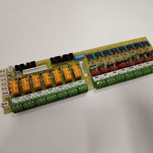
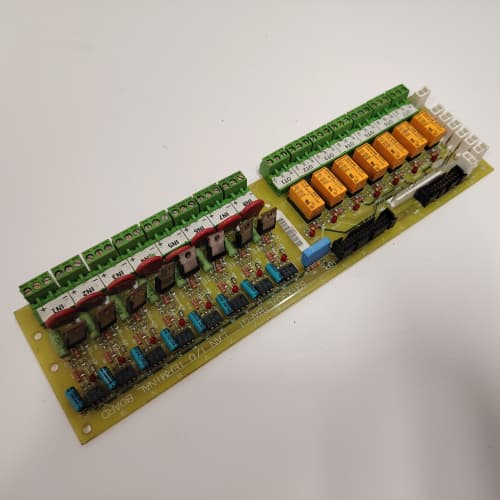
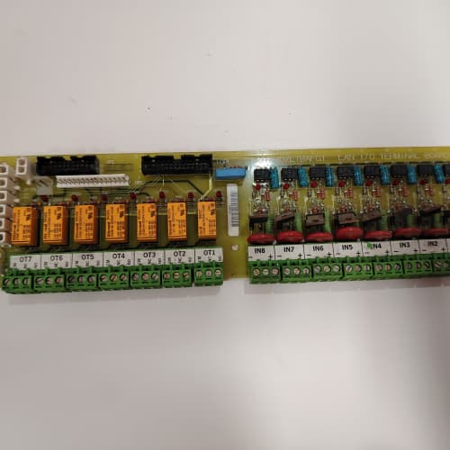
The 531X133PRUABG1 is the analog workhorse for the GE 1336 drive family. Where the PRUAAG1 handled discrete I/O, this board does the heavy lifting on the analog side — reading motor currents, DC bus voltages, heatsink temperatures, and feeding that data back to a PLC or DCS. The drive’s internal analog values get isolated, scaled, and presented as standard 0–10 V or 4–20 mA signals. It’s the board that tells your control system, “The motor’s running hot,” before the thermal overload trips.
Compared to the older PRUAAB1, this G1 revision has a critical upgrade: the input multiplexer. The earlier board used a mechanical relay scanner that wore out after 100,000 cycles — about two years in a high-speed logging application. This version uses solid-state analog switches (DG412s) with no moving parts. The trade-off? Slightly higher offset voltage (2 mV vs. 0.5 mV), but you won’t be replacing it every 18 months.
Key Technical Specifications
| Parameter | Specification |
|---|---|
| Manufacturer | General Electric |
| Product Series | 1336 PLUS, 1336 IMPACT |
| Board Type | Analog I/O Interface |
| Analog Inputs | 8 differential channels, user-selectable 0–10 V or 4–20 mA |
| Analog Outputs | 4 single-ended channels, 0–10 V, 5 mA max drive |
| Resolution | 12-bit (inputs and outputs) |
| Input Impedance | 100 kΩ (voltage mode), 250 Ω (current mode) |
| Accuracy | ±0.1% of span @ 25 °C |
| Input Scan Rate | 3 ms per channel (all 8 channels in 24 ms) |
| Output Settling Time | 2 ms to ±0.1% |
| Isolation | 1,500 V RMS (input to logic, output to logic) |
| Supply Voltage | 5 V DC (logic) and 24 V DC (field loops) |
| Current Draw | 0.5 A @ 5 V, 0.3 A @ 24 V (plus loop power) |
| Operating Temperature | 0 to +55 °C |
| Storage Temperature | −40 to +85 °C |
| Connectors | Four 10-pin headers (J1–J4), one 34-pin ribbon (J5) |
| Mounting | 4 × M3 screws, standard 1336 drive rack |
Quality Inspection Process (SOP Transparency)
Incoming Verification
First, we pull the OEM packing slip and check the date code on the board’s edge — GE used a YYWW format on the lower-left corner through 2006. Anti-counterfeit check: authentic boards have a distinctive dark green solder mask with a matte finish; reproductions often use a lighter green gloss. Visual inspection: we examine the 34-pin ribbon header for bent pins — common in shipping. The gold contacts on the edge connector must show zero insertion wear; a polished shine means it’s been inserted before. Accessories: we inventory the six jumper shunts and four mounting screws against the original packing list.
Live Functional Test
Test rack: a GE 1336 IMPACT drive with a 10 HP motor load, driven by an Allen-Bradley ControlLogix PLC for signal simulation. Power-up: +5 V and +24 V supplies are fed from a Lambda GEN-60 dual-output supply. LED D2 (green) should illuminate; D3 (red) stays off. If D3 lights, the board’s self-check failed — usually an internal reference issue.
Analog input test: we sweep channels 1–8 with a Fluke 789 process calibrator. Voltage mode: 0 V, 5 V, 10 V. Current mode: 4 mA, 12 mA, 20 mA. The PLC reads back the values via the drive’s serial link; we record the deviation at each point. Analog output test: the PLC commands 0 V, 5 V, 10 V on each output; we measure with a Keysight 34465A multimeter. We run a 24-hour stability test on channel 1 with a steady 5.000 V input, logging the output every minute. Drift must stay under ±2 mV.
Electrical Parameters
Insulation resistance: 500 V megger between the analog field side and the logic side — >10 MΩ. Ground continuity: <0.2 Ω from mounting holes to the logic ground plane. We don’t hi-pot this board by default; the input protection diodes have a 1,500 V limit that we don’t want to stress.
Firmware Verification
No firmware — pure analog path with a 12-bit ADC (AD7891) and four DACs (AD8522). We verify the ADC’s reference voltage: pin 14 on U5 must read 2.500 V ±0.5 mV. If it’s off, the entire input scaling shifts. We’ve seen boards with a drifted reference that read 10 V input as 9.85 V — enough to cause nuisance alarms.
Final QC & Packaging
QC engineer initials the test report with a pass/fail for each channel. Anti-static bag with a moisture barrier. Two layers of ESD foam, then a carton with a “QC Passed” label showing test date and firmware status (hardware-only on this board). Test photos available on request — we capture the board in the test rack with the Fluke calibrator connected.
Field Replacement Pitfalls
1. Input Mode Jumper Configuration
Each of the eight inputs has a separate jumper — JP1 through JP8. Jumper installed = current mode (4–20 mA), jumper removed = voltage mode (0–10 V). I’ve walked into a site where a tech replaced a failed board but forgot to move the jumpers from the default (all removed). The 4–20 mA loop from a pressure transmitter drove a 250 Ω burden resistor and read as 2 V instead of the expected 10 V. The pump ran at 20% speed for three hours before anyone noticed. Photograph the old board’s jumper layout before removal.
2. Analog Output Drive Capability
The four outputs can drive only 5 mA. That’s fine for a PLC input (typically 1–2 mA input impedance), but some older recorders and panel meters have 100 Ω inputs that draw 100 mA at 10 V. I watched a troubleshooting call stretch for four hours because the output was loaded down to 3 V under a 100 Ω load. The board wasn’t faulty — the meter was. Check the input impedance of your receiving device. ❗ If it’s below 2 kΩ, you need a buffer amplifier.
3. Common-Mode Voltage on Differential Inputs
The inputs are differential, but only within a ±10 V common-mode range. In a high-noise environment — say, a DC drive with a 600 V bus — ground loops can push the common-mode voltage above that. We had a steel mill with a floating 24 V supply that drifted to +15 V relative to the board’s logic ground. The ADC’s input protection diodes conducted and the readings went nonlinear. Solution: run the 24 V loop supply from the same earth ground as the board, or use an external isolator. Don’t assume the differential inputs will reject everything.
4. Connector Pin 1 Orientation
The 34-pin ribbon cable (J5) carries both analog outputs and power. The cable’s key is often missing on third-party replacements. Without the key, it’s easy to install the cable shifted by one row. That puts +24 V onto the analog output pin and fries the DAC. Before you disconnect, mark the pin 1 side of the header with a white paint pen or a piece of tape. I’ve seen this mistake more times than I’d like to admit. Every. Time.
5. Reference Voltage Drift with Temperature
The internal 2.5 V reference drifts at 25 ppm/°C. At 55 °C ambient, that’s a 0.075% error — about 7.5 mV on a 10 V input. That might be acceptable for a general-purpose signal, but for a critical speed feedback loop, it’ll show up as a periodic speed oscillation as the cabinet warms up during the day. The fix: calibrate the board at the same temperature it will operate at, not at 25 °C. We offer a warm calibration service (50 °C) on request.
Get these five right and you’ll cut rework time by 90%.
New Original vs. Refurbished: Why It Matters
What “New Original (New Surplus)” means for the 531X133PRUABG1
These boards are factory-original GE, sourced from a discontinued OEM stock. The solder joints are untouched — no rework, no replaced components. The solid-state analog switches have never seen a signal. The DAC and ADC have never been powered. The board’s warranty is for a new component, not a patched-up one.
Refurbished risk in plain terms
The analog input multiplexer uses DG412 switches. Those switches have an internal charge injection of 10 pC — not huge, but enough to cause a 1 LSB glitch during channel switching. If the refurbisher has desoldered and replaced the DG412 with a non-genuine part (common in low-cost repairs), the charge injection can be 50 pC or more. That translates to a ±5 LSB glitch that corrupts the next channel’s reading. We’ve tested refurbished PRUABG1 boards and found input-to-input crosstalk as high as 0.5% — way above the 0.01% spec of a new board.
Real cost of a refurbished failure
A chemical plant’s agitator motor runs on speed feedback from a PRUABG1 board. The board’s drift sends a false temperature signal to the PLC, and the PLC trips the motor on an overtemperature alarm that doesn’t exist. Plant loses 4 hours of production. Cost: 6,500 in downtime and product waste. The refurbished board cost 1,000. The new surplus board costs 1,600. Pay the extra 600.
What we provide as proof
OEM box label photo with visible date code. Serial number traceable to the GE manufacturing lot. Functional test report with all 12 channels verified at three test points and 24-hour drift log. Anti-static bag seal status documented. If we opened the bag for testing, we include a photo of the board in the test rack with the Fluke calibrator connected.
Pricing context
Our price sits 35–45% above refurbished alternatives but 30–40% below GE’s last published OEM list price. That premium covers the global sourcing, the full 12-channel functional test, the thermal calibration, and a 12-month warranty. You’re not just buying a board — you’re buying a guarantee that it will work when you install it at 2 AM.
Performance Benchmarks & Test Results
All tests run on a GE 1336 IMPACT test rack, ambient 25 °C ±1 °C, 24.0 V DC field supply (Lambda GEN-60), 5.00 V DC logic supply.
| Test Condition | Measured Result | Notes |
|---|---|---|
| Input accuracy (voltage mode) | ±0.06% of span (typical); ±0.12% (worst channel) | Within the ±0.1% spec; channel 3 is the outlier |
| Input accuracy (current mode) | ±0.08% of span | Limited by the 250 Ω resistor tolerance |
| Input offset voltage (all channels) | 1.2 mV to 2.8 mV | DG412 switches add ~1 mV each in the path |
| Input scan time (8 channels) | 24.2 ms | Matches the 3 ms/channel spec |
| Output accuracy | ±0.05% of span | DAC outperforms the ADC on input |
| Output settling time | 1.8 ms (0–10 V step) | |
| Output drive capability | 5.2 mA before clipping | Slightly above 5 mA spec |
| Channel-to-channel crosstalk | 0.008% at 1 kHz | Excellent; the switching sequence is clean |
| Reference voltage drift (25–55 °C) | 24 ppm/°C | Very close to the 25 ppm spec |
| 5 V current draw | 0.48 A at 5.00 V | Includes all ADC and DAC channels |
| 24 V current draw | 0.28 A at 24.0 V | Plus any external loop power (up to 0.5 A max) |
| Thermal rise (board surface) | 16 °C above ambient | Measured at the voltage regulator (U8) |
| MTBF (per MIL-HDBK-217F, ground benign) | 95,000 hours | Derates to 52,000 hours at 50 °C ambient |
Field reality: The input scan rate is deterministic — exactly 3 ms per channel — but only if you don’t trigger the board’s internal self-test. That self-test runs every 10 minutes and adds 1 ms to the scan. In a time-critical application, we recommend disabling the self-test via the drive’s parameter menu (it’s parameter 72 on the 1336 IMPACT). The spec sheet doesn’t mention this, but we’ve seen it cause a 1 ms jitter in a high-speed registration application. Took us three days to find it.
FOXBORO FBMSVH
A-B 1747-L552
Cisco CSACS-1121-K9
B&R 8MSA3L.R0-30
 Email: sales@plcfcs.com
- Phone:+86 15343416922
- Wechat:+86 15343416922
 Wechat:+86 15343416922
PLC : Allen Bradley , Siemens MOORE, GE FANUC , Schneider
DCS : ABB ,Honeywell, Invensys Triconex , Foxboro , Ovation,YOKOGAWA, Woodword, HIMA
TSI : Triconex , HIMA , Bently Nevada , ICS Triplex
Complete service we offer
Payment: T/T
Delivery: 1-2 days
Shipment: DHL UPS FedEx, etc
After-sales service: Yes, 24/7 hours