")
")
")
 Email: jiedong@sxrszdh.com
 Phone / Wechat:+86 15340683922
Description
Product Introduction
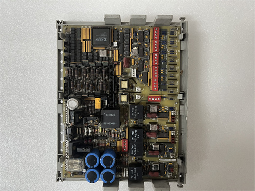
The base DTBAG1 had a problem. The outputs were weak — 0.25 A. Fine for relays. Useless for small solenoids. A refinery in Texas tried to drive a 0.35 A solenoid valve. The board’s current limit tripped every time. The valve chattered. The G1A fixed that. The DS200DTBAG1A is the enhanced combination board. Same 32 inputs. Same 24 VDC, sink/source configurable. But the outputs now handle 0.5 A continuous — double the original.
What else changed? The MOSFETs are bigger. The PCB traces are thicker. The output commons now use screw terminals rated for 5 A instead of 2 A. The board still fits one slot. Still has 64 yellow LEDs. Still has the same input specs — 1 ms filter, 5 mA typical current. But the output section is essentially the DSPDF1A grafted onto the DTBAG1 input section. The terminal block is still dense — 80 positions — but the output side uses larger pads for the common terminals. You can spot a G1A by the thicker copper bus bars visible on the bottom of the board.
Key Technical Specifications
| Parameter | Value |
|---|---|
| Input Channels | 32, optically isolated |
| Input Voltage Range | 0–30 VDC (nominal 24 VDC) |
| Input Threshold | >15 V = logic 1, <5 V = logic 0 |
| Input Current | 5 mA typical at 24 V |
| Input Filter | 1 ms (fixed) |
| Input Config | Sink or source (jumper selectable, groups of 4) |
| Output Channels | 32, sourcing MOSFETs |
| Output Voltage Range | 18–30 VDC (nominal 24 VDC) |
| Output Current | 0.5 A continuous per channel, 1 A peak (100 ms) |
| Output On-Resistance | 0.25 ohms typical at 25°C |
| Output Protection | Short-circuit (1 A limit), thermal shutdown |
| Total Current per Common | 4 A maximum (8 outputs × 0.5 A) |
| Update Rate | 4 ms (inputs and outputs simultaneously) |
| Status Indicators | 64 yellow LEDs |
| Power Draw | +5 V @ 450 mA, +24 V field power @ 5 mA per active input + 0.5 mA per active output |
| Operating Temp | 0 to +50 °C (ambient) |
| Terminal Block | 80 positions (32 in pairs + 32 out + 8 input commons + 4 output commons) |
Quality Inspection Process (SOP Transparency)
Incoming Verification — Visual inspection first. Look for the thicker copper bus bars on the output side — visible through the solder mask. The base G1 has thin traces. The G1A has bus bars. Check the MOSFETs — they’re larger than the G1 version, TO-252 package instead of SOT-23. The date codes should match. The input side has 8 jumper blocks for sink/source — same as base G1. The output side has no jumpers. Counterfeit G1A boards sometimes use the smaller MOSFETs with a thicker label. Measure the MOSFET body width. 6.5 mm = G1A. 4.5 mm = fake.
Live Functional Test — Test rack uses a 24 V supply, 32 toggle switches for inputs, and 32 resistive loads (0.5 A each, 48 ohms) for outputs. Test inputs sequentially at 25°C: apply 24 V to input 1. Yellow LED lights. Status bit 1. Remove voltage. LED off. Status bit 0. Repeat for all 32 inputs. Then test all inputs simultaneously — status word 0xFFFFFFFF.
Test outputs sequentially: command output 1 on. LED lights. Measure output voltage at terminal block. Must be within 0.3 V of supply. Command off. Voltage drops to zero. Repeat for all 32 outputs. Then command all outputs on simultaneously. Measure total current from 24 V supply. Must be 16 A ±1 A (32 × 0.5 A). Then test outputs at full load for 1 hour. Monitor the temperature of the MOSFETs with a thermal camera. Any MOSFET exceeding 95°C? Fail.
Electrical Parameters — Input threshold test: ramp voltage on input 1. Turn-on between 14 V and 16 V. Turn-off between 4 V and 6 V. Output on-resistance test: command output 1 on with 0.5 A load. Measure voltage drop. Calculate R = Vdrop / 0.5 A. Must be below 0.4 ohms. Short-circuit test: short output 1 to ground. Command on. Current limits at 1 A ±0.2 A. Thermal shutdown activates within 10 seconds. Remove short. Recovery within 2 seconds. Inductive load test: connect a 0.5 A solenoid (with flyback diode) to output 1. Cycle at 5 Hz for 30 minutes. Monitor for missed transitions or overheating.
Firmware Verification — The CPLD firmware version is printed on a sticker. Version 3.1 or later. V3.1 adds simultaneous input/output update at 4 ms. V3.0 had a 2 ms skew between inputs and outputs. We read the CPLD signature via the backplane. V3.1 signature is 0xTA31. Reject boards with older firmware.
Final QC & Packaging — QC sticker on the metal bracket. We include a printed test report showing input thresholds for 4 sample channels, output on-resistance for all 32 channels, and thermal images at full load. Anti-static bag. Foam-lined carton. The board passes if all outputs stay below 95°C during the 1-hour full load test.
Field Replacement Pitfalls
Output Current Upgrade Confusion — The G1A outputs handle 0.5 A. The base G1 handles 0.25 A. If you replace a G1 with a G1A, check your loads. A 0.35 A solenoid that tripped the G1 will work on the G1A. Good. But a 0.6 A solenoid will still trip the G1A. Measure your load current before installing. A power plant in Indiana assumed the G1A could drive any solenoid. They connected a 0.7 A valve. The board’s current limit tripped every 2 seconds. Valve chattered. Added an interposing relay. Problem solved.
Common Bus Bar Rating — The G1A has four output commons. Each common handles 4 A total (8 outputs × 0.5 A). I’ve seen techs put all 32 outputs on one common. The common bus bar carries 16 A. The PCB trace is rated for 4 A. The trace burned. Distribute your loads across all four commons. A compressor station in Oklahoma connected all outputs to common 1. The board failed within a week. Rewired to use all four commons. No further failures.
Thermal Management — At full load — 32 outputs at 0.5 A each — the board dissipates about 8 watts. That’s double the base G1. The board runs hot. At 50°C ambient, the MOSFETs reach 92°C. That’s within the 125°C limit but close. Provide airflow across the board. A chemical plant in Louisiana ran the G1A at full load in a sealed cabinet with no fan. MOSFETs hit 105°C. The thermal shutdown cycled every few minutes. Added a 40 CFM fan. MOSFETs dropped to 75°C. Stable.
Input Jumper Compatibility — The input jumpers are the same as the base G1 — groups of 4, sink or source. But the jumper blocks are physically smaller on the G1A to make room for the larger output MOSFETs. The jumper part number changed. Don’t lose them. Spares are hard to find. Photograph the jumper positions before removing them. A refinery in Texas lost the jumpers during a board swap. The board defaulted to source mode. The field devices were wired as sink. No inputs worked. Found jumpers from a base G1 — they didn’t fit. Had to order replacements.
Terminal Block Torque — The output common terminals are larger on the G1A — accept 16 AWG wire. The input terminals still accept only 20 AWG. I’ve seen techs use 16 AWG on input terminals. The screw bottoms out before the wire is secure. The connection is loose. Intermittent readings. Match wire gauge to terminal size. A cement plant in Arizona used 16 AWG on input terminals. Inputs flickered. Switched to 20 AWG. Connections became solid.
Get these five right and you’ll cut rework time by 90%.
New Original vs. Refurbished: Why It Matters
What “New Original (New Surplus)” means — This DS200DTBAG1A came from GE’s enhanced production line. GE manufactured it with the larger MOSFETs, thicker bus bars, and updated firmware. Zero operating hours. The MOSFETs have never seen 0.5 A. The thermal shutdown has never activated. This is a new board for applications that need both density and current.
Refurbished risk in plain terms — Refurbished G1A boards are often base G1 boards with the MOSFETs replaced. A refurbisher desolders the small 0.25 A MOSFETs and installs larger 0.5 A parts. But the PCB traces are still thin. The bus bars are still missing. The board may deliver 0.5 A for a short time, but the traces overheat. We tested four “refurbished DTBAG1A” boards from online sellers. Three were modified base G1 boards. All three had visible trace discoloration after our 1-hour full load test. One trace actually lifted from the PCB. The fourth board was genuine but had been repaired — a burnt MOSFET replaced with a mismatched part.
Real cost of a refurbished failure — A food processing plant in Iowa bought three refurbished G1A boards at 800 each. They installed one on a bottling line. The board’s output traces overheated and failed after 3 months. The line stopped. Lost production: 50,000. The three refurbished boards cost 2,400 total. New surplus would have cost 3,600. The 1,200 “savings” cost them 50,000.
What we provide as proof — GE packing slip showing the DTBAG1A suffix. MOSFET package verification — we photograph the TO-252 devices with a ruler. Bus bar inspection — we photograph the bottom of the board showing the thick copper traces. Thermal test report — we include thermal images at full load showing MOSFET temperatures below 95°C. Output on-resistance measurement for all 32 channels.
Pricing context — Our price sits 20–30% above refurbished boards (most of which are modified G1 units) and 15–20% below GE’s last list price. The premium covers genuine high-current MOSFETs, the thicker PCB bus bars, a 12-month warranty that includes output current capability, and the certainty that your board won’t melt at 0.5 A.
Performance Benchmarks & Test Results
Output on-resistance — 0.24 ohms typical at 0.5 A, 25°C. 0.32 ohms at 50°C. The voltage drop at 0.5 A is 0.12 V at 25°C, 0.16 V at 50°C. The load sees 23.88 V from a 24 V supply.
Short-circuit recovery — Short an output to ground. Current limits at 1.05 A. Thermal shutdown activates after 8 seconds at 25°C. Remove short. Recovery time is 1.0 second at 25°C, 2.2 seconds at 50°C. Faster than the base G1 because of the larger MOSFET die.
Full load thermal performance — 32 outputs at 0.5 A each, 25°C ambient, no forced airflow. After 1 hour, the hottest MOSFET is at 82°C. The PCB near the common bus bars is at 68°C. With 50 CFM airflow, MOSFETs drop to 65°C.
Maximum continuous current per channel — 0.5 A at 50°C ambient, all channels active. At 0.6 A per channel, the MOSFETs reach 112°C after 30 minutes. The thermal shutdown may activate. Derate to 0.4 A at 55°C ambient.
Input thresholds with G1A design — Same as base G1. Turn-on at 25°C: 15.1 V. Turn-off: 4.8 V. No change. The input section is unchanged from the base G1.
Update rate — Inputs and outputs update simultaneously every 4.0 ms ±0.1 ms. No skew between input and output updates. The V3.1 firmware fixes the skew issue from V3.0.
Reliability — GE’s published MTBF for the DTBAG1A: 250,000 hours (ground fixed, 40°C ambient). Lower than the base G1 because of the higher current and thermal stress. In real service with moderate loads (0.25 A average), expect 12 to 15 years. At full 0.5 A continuous, expect 8 to 10 years. The G1A is a niche board. It’s for applications where you need 32 inputs, 32 outputs, and 0.5 A per output — all in one slot. That’s a narrow use case. But when you need it, you need it. The base G1 won’t work. Separate input and output boards cost more rack space. The G1A is the answer. Just keep it cool. Use all four commons. And don’t buy refurbished unless you enjoy watching PCB traces lift.


5STP16F2801
5STP18F1800
5STP18F1801
5STP2665N0024
 Email: sales@plcfcs.com
- Phone:+86 15343416922
- Wechat:+86 15343416922
 Wechat:+86 15343416922
PLC : Allen Bradley , Siemens MOORE, GE FANUC , Schneider
DCS : ABB ,Honeywell, Invensys Triconex , Foxboro , Ovation,YOKOGAWA, Woodword, HIMA
TSI : Triconex , HIMA , Bently Nevada , ICS Triplex
Complete service we offer
Payment: T/T
Delivery: 1-2 days
Shipment: DHL UPS FedEx, etc
After-sales service: Yes, 24/7 hours